民恩滤波器 解决您设备的干扰! 如有需要请您联系《上海民恩电气有限公司》咨询!
民恩滤波器 解决您设备的干扰! 如有需要请您联系《上海民恩电气有限公司》咨询!
通过图①所示,为减小接地阻抗,滤波 器应安装在导电金属表面或通过编织接地带 与接地点就近相连,避免细长接地导线造成 较大的接地阻抗。
如图②所示,安装的地方应选在电源入口 处缩短输入线在机箱内的长度,减少辐射干 扰。
5. 布线 滤波器的输入线与输出线不得平行或交叉;应使输入、输出线. 检查 每年应最少一次对滤波器的连接进行检查。
EMI电源滤波器概述EMI(Electromagnetic Interference)电源滤波器是一种用于减小电源传导和辐射的电磁干扰的设备。
滤波器安装前请先阅读此需要注意的几点!!! 1. 测试 上海民恩电气有限公司的每一只产品在出厂前均经过严格的测试,
过载电流 Overload current 开机瞬间允许通过4倍过工作电流,1.4倍工作电流1分钟(每小时一次)
上海民恩电气有限公司 GB/T7343-87《10kHz-30MHz 无源无线电干扰滤波器和抑制元件 抑制特性的测量方法》及 UL1283《电磁干扰滤波器》标准制定
上海民恩电气有限公司 GB/T7343-87《10kHz-30MHz 无源无线电干扰滤波器和抑制元件

1、变频器滤波器是基于变频器在工作时,对电网及其它数字电子设备产生干扰的频谱分量电磁兼容 性特点而专门设计的。
2、安装于电机和变频器及电源与变频器之间。 3、小尺寸,无需风扇,采用的是经过最恶劣环境测试过的高性能的材料和部件。 变频器滤波器参数
如果变频器的输入端三相不平衡,严重的情况下,就会导致变频器无法正常工作,加上变频器
变频器专用输入EMC滤波器,主要是由(L)滤波电感、(C)滤波电容和(R)电阻构成。
打开试气开关(5),电流表(19)显示所设定的电流值 拨动下坡电流时间设置开关(6),在电流表(19)上读 取设定值(ms) 在“1”位置(首选值) 控制: 更换消耗件后吹干割枪 黄色错误统计指示灯(16)“亮” 电压表(20)显示“gas” 调整到切割表要求的引弧高度 在工件上穿孔 HiFocusF 技术启动 割枪开始工作: 在辅助弧接触到工件后辅助弧指示灯(10)“亮” 主弧指示灯(11)“亮” 切割工作
--更换消耗件时,请务必断开电源开关。 --其他零部件禁止操作员更换。 --仅能使用凯尔贝原装消耗件,否则担保无效。 --消耗件,割枪头必须远离易燃易爆环境,如有油或油脂等环境。 --按照切割技术方面的要求(切割表),确保割枪装入正确的消耗件。 --确认装好消耗件后,用吹气功能吹干枪头里的水。
卸下消耗件步骤如下: 1.手工或者用钩行扳手(62.07)旋下涡流帽(3x.12)。 2.手工旋下保护帽(3x.11),连同涡流喷嘴(3x.09)。(从保护帽上可以取下涡流喷嘴) 3.用扳手(62.04)旋下喷嘴帽(3x.07)。 4.取出喷嘴(3x.05)。 5.使用涡流环拉手(62.03)从喷嘴中拉出涡流环(3x.03)。(等离子空气,氧气都适用) 6.使用扳手(62.02)旋出电极(3x.02)。 7.用六角扳手(62.05)旋出冷却水管(3x.01)。
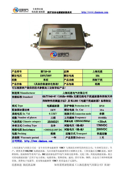
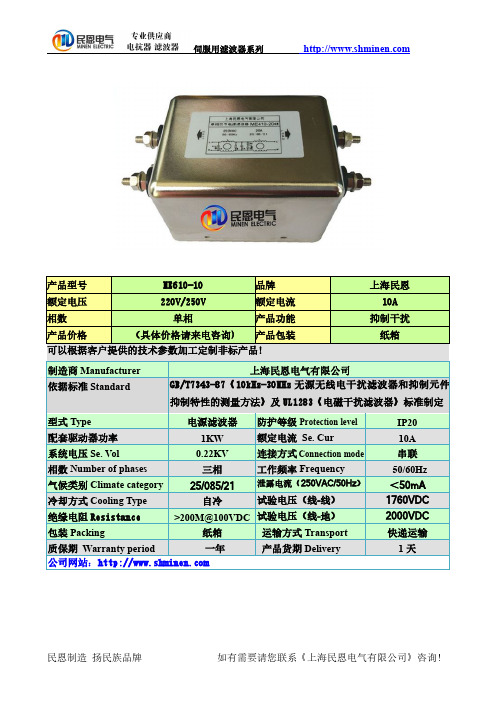
上海民恩电气有限公司是一家专门干电磁兼容(EMC)与谐波技术探讨研究的科技公司。专业研发设计、生 产、销售各种 EMI/EMC 电源滤波器,为公司可以提供电磁兼容的全面解决方案,工程实施以及 EMI 滤波、脉冲 群抑制、浪涌抑制等系列新产品。EMI 滤波器包括军用/工业级交流单相、交流三相、直流电源滤波器。我公 司的电源滤波器大范围的使用在电力系统、电源系统、变频系统、通讯、医疗设施、钢铁、冶金及工业控制检测 设备、消费电子电器等,是实现电磁兼容(EMC)的首选电子元器件。

交流单相电源滤波器双节增强型ME610系列◆ 产品及应用● 双节滤波器,极强的差模滤波效果 ● 具有差模滤波电感 ● 低频性能优异● 适用于开关电源、逆变、伺服、电源转换器等单相工业设施等控制管理系统ME610系列◆ 技术参数标称电压 250VAC额定电流@40℃1A~25A 试验电压线◆ 产品列表产品型号额定电流 @40℃ 泄露电流 250VAC/50Hz 外型电路参数端接方式重量(g )L (mH)L1 (uH) Cx (uF) Cy (nF) R (MΩ)ME610-1 1A ≤0.3mA H1 11.0 280 0.22 2.2 1.0 L M4 160 ME610-3 3A ≤0.3mA H1 6.5 150 0.22 2.2 1.0 L M4 160 ME610-6 6A ≤0.5mA H2 2.8 90 0.22 4.7 1.0 L M4 230 ME610-10 10A ≤0.5mA H5 2.5 70 0.47 4.7 0.47 L M4 300 ME610-16 16A ≤0.5mA J 1.5 45 1.0 4.7 0.22 L M4 400 ME610-2525A≤0.5mAJ1.2201.04.70.22--- M6400◆ 电路原理图◆ 插入损耗 (PER CISPR 17; A=50/50ΩSym)LINE TO GROUND(PN---E)共模 (dB)LINE TO LINE(P---N)差模 (dB) MHz .1 .15 .5 1 5 10 30 .1 .15 .5 1 5 10 30 ME610-1 44 50 67 69 59 52 52 67 80 87 90 80 72 60 ME610-3 35 37 58 67 83 75 52 55 68 72 77 82 70 49 ME610-6 25 28 61 56 53 59 40 50 65 78 72 76 62 53 ME610-10 25 28 55 50 60 68 55 43 50 73 77 75 78 72 ME610-16 18 20 35 42 50 55 58 40 50 75 76 69 75 65 ME610-◆外观尺寸(mm)上海民恩电气有限公司。
本产品样本中包含的产品和系统是 根据 DQS 认证的质量管理体系按 照 DIN EN ISO9001 标准制造的 (认证注册编号:FM25845)。DQS 认证得到了所有 EQ Net 国家的承 认 (注册号:FM25845)
MICROMASTER 440 “适用于一切传动装置” 具有高级的矢量控制功能 (带有或不带编码器反馈),可用于多种部 门的各种用途,例如传送带系统,纺织机械,电梯,卷扬机以及建 筑机械等。
通用变频器应用资料: 1. 通用变频器驱动装置在化工企业搅拌机上的应用 2. 变频调速恒压供水在陕西兴平化肥厂的应用

MIC4834Low Noise Dual 220 V PP EL DriverMLF and Micro Lead Frame are registered trademark of Amkor TechnologiesMicrel Inc. • 2180 Fortune Drive • San Jose, CA 95131 • USA • tel +1 (408) 944-0800 • fax + 1 (408) 474-1000 • General DescriptionThe MIC4834 is a low noise dual Electroluminescent (EL) Panel driver used in backlighting applications. The MIC4834 converts a low DC voltage to a high DC voltage using a boost converter and then alternates the high DC voltage across the EL panels using an H-bridge. The MIC4834 incorporates internal wave-shaping circuitry specifically designed to reduce audible noise emitted by EL panels. With only one inductor the MIC4834 can drive two outputs and requires a minimum number of passive components. It features an operating input voltage range of 2.3V to 5.8V, making it suitable for 1-cell Li-ion and 2- or 3-cell alkaline/NiCad/NiMH battery applications.The MIC4834 features separate oscillators for the boost and H-bridge stages. The boost frequency may be adjusted with an external resistor to optimize efficiency and brightness. The H-bridge frequency is internally preset to 225Hz, to reduce the number of external components and layout space.The MIC4834 is available in 10 pin 3mmx3mm MLF package as well as MSOP-10L, and has an operating junction temperature range of –40C to +125C.Features•Drives two EL panels, up to 3 in 2 each at full brightness• 220V PP regulated AC output waveform • 2.3V to 5.8V DC input voltage• Wave-shaping circuit to reduce audible noise • Adjustable boost converter frequency • Single inductor to power both panels • 0.1A typical shutdown current • Package options− 10-pin 3mmx3mm MLF − 10-pin MSOP• –40oC to +125o C junction temperature rangeApplications• Mobile phones• MP3/portable media players (PMP) • Clocks/ watches • Remote controls • Cordless phones • GPS devices • PDAs_________________________________________________________________________________________________Typical ApplicationLow Noise Dual EL DriverOrdering InformationPart Number Package Operating Junction Temp RangeLead Finish MIC4834YML10 pin (3mm x 3mm) MLF-40C to +125C Pb-free / RoHS-CompliantMIC4834YMM 10-Pin MSOP -40C to +125C Pb-free / RoHS-Compliant Pin Configuration10-Pin MLF - Top View 10-Pin MSOP – Top ViewPin DescriptionPin Number Pin Name Pin Function1 ENA EL Panel A Enable Pin: Logic high enables ELA and logic low disables ELA output.2 VDD DC Input Supply Voltage: 2.3V to 5.8V3 RSWRSW pin: Sets internal boost converter switch frequency by connecting an externalresistor (R SW) to VDD. Connecting the R SW resistor to GND shuts down the device.4 ENB EL Panel B enable pin: Logic high enables ELB and logic low disables ELB output.5 GNDGround.6 SW Switch Node: Drain of internal high-voltage power MOSFET for boost circuit.7 CSRegulated Boost Output: Connect to the output capacitor of the boost regulator andto the cathode of the diode.8 COMEL output: Common EL output terminal to both ELA and ELB. Connect one end ofeach EL panel to this pin.9 ELB EL Panel B output: Connect the other end of the EL panel B to this pin.10 ELA EL Panel A output: Connect the other end of the EL panel A to this pin.EPad HS Pad Heat Sink Pad. Connect to ground externally. MLF package only.Absolute Maximum Rating(1)Supply voltage (V DD).......................................-0.5V to 6.5V Output voltage (V CS)...................................... -0.5V to 130V Switch Node (V SW).........................................-0.5V to 130V Enable Voltage (V RSW, V ENA, V ENB)...................-0.5V to 6.5V Ambient Storage Temperature (T S) ...........-65C to +150C ESD Rating(3)...........................................................................ESD Sensitive Operating Range(2)Supply Voltage (V DD)........................................2.3V to 5.8V Switching MOSFET Frequency (f SW)........35kHz to 350kHz Enable Voltage (V RSW, V ENA,,V ENB).......................0V to V DD Junction Temperature Range (T J).............-40C to +125C Package Thermal Impedance3mm x 3mm MLF (θJA)……………………........60C/W MSOP(θJA)…………………….........................206C/WElectrical Characteristics(4)T A = 25o C, V DD= 3.0V unless otherwise noted. Bold values indicate -40C ≤ T J≤ 85C.Symbol Parameter Condition Min Typ Max UnitsV DD Supply Voltage Range 2.3 5.8 VI DD InputSupplyCurrent V RSW = High; V CS = 105V;ELA, ELB, COM = Open152 220 AI SD ShutdownCurrent V RSW = Low; V DD = 5.8V 0.1 1 AR DS(ON) On-resistance Of Switching Transistor I SW = 100mA, V CS = 105V 6.0 12.0 ΩV CS Output voltage Regulation V DD = 2.3V to 5.8v 90 109 120 VV DD = 3.0V(R SW = 1.3MΩ )25 35 45 kHzV DD = 3.0V (R SW = 450kΩ) 75 100 125 kHzf Sw Boost Switching FrequencyV DD = 3.0V(R SW = 125kΩ)250 350 450 kHzf EL ELA, ELB and COM Drive Frequency V DD = 3.0VELA, ELB, COM = Open165 225 285 HzD Switching Transistor Duty Cycle 80 95 %I OUT Output Current Drive Limit 2.5 5 7.5 mAV ENA,V ENBEnable Logic Threshold 0.4 1.2 VV HYS Enable Logic Hysteresis 20 50 150 mVI ENA,I ENBEnable Input Current 0.1 1 A Notes:1. Exceeding the absolute maximum rating may damage the device.2. The device is not guaranteed to function outside its operating rating.3. Devices are ESD sensitive. Handling precautions recommended. Human body model, 1.5kΩ in series with 100pF.4. Specification for packaged product only.Typical CharacteristicsFunctional DiagramFigure 1. MIC4834 Block Diagram Functional DescriptionOverviewThe MIC4834 is a high-voltage dual output EL driver with a peak-to-peak AC output voltage of 220V capable of driving two 3 in2 EL panels. The MIC4834 drives EL panels by converting a low DC input voltage to a high DC high output voltage using the boost regulator circuit and then alternating the high DC voltage across the EL panel using an H-Bridge. Input supply current for the MIC4834 is typically 152A. The high voltage EL driver has two internal oscillators to control the boost switching frequency and the H-bridge driver frequency. The internal boost oscillator frequency can be individually programmed through an external resistor to maximize efficiency and brightness of the EL panel. The H-bridge frequency is internally fixed at 225Hz to reduce external component count.R egulationReferring to Figure 1, power is initially applied to V DD. When the internal feedback voltage is less than the reference voltage, the internal comparator enables switching in the boost circuit. When the boost regulator is switching, current flows through the inductor into the switch. The switching MOSFET will typically turn on for 90% of the switching period. During the on-time, energyis stored in the inductor. When the switching MOSFET turns off, current flowing into the inductor forces the voltage across the inductor to reverse polarity. The voltage across the inductor rises until the external diode conducts and clamps the voltage at V OUT + V D1. The energy in the inductor is then discharged into the C OUT capacitor. The internal comparator continues to turn the switching MOSFET on and off until the internal feedback voltage is above the reference voltage. Once the internal feedback voltage is above the reference voltage, the internal comparator disables switching. The control circuit will continue to turn the MOSFET’s on and off to maintain a constant DC voltage at the CS pin.When the MIC4834 EL Driver is enabled, ELA and ELB will switch in opposite states with COM to achieve a 220V peak-to-peak AC output signal needed to drive the two EL panels.Switching FrequencyThe switching frequency of the converter is controlled by an external resistor (R SW ) between RSW and VDD. The switching frequency increases as the resistor value decreases. In general, the lower the switching frequency, the greater the input current is drawn to deliver more power to the output. Lowering the switching frequency can be used to drive larger panels. However, the switching frequency should not be so low as to allow the voltage at the switch node or the CS pin to exceed the absolute maximum voltage of those pins. For resistor value selections, see the “Typical Characteristics: Switching Frequency vs. SW Resistor” graph on Page 4 or use the equation below. The switching frequency range is 35kHz to 350kHz, with an accuracy of 20%.()Ω=M R 46(kHz)f SW SWEL FrequencyThe MIC4834 EL panel frequency is internally fixed at 225Hz.Enable FunctionThere are a few different ways to enable and disable the MIC4834. The boost regulator may be disabled by pulling the R SW resistor to ground. This turns off both the EL panels by cutting power to the device completely. The R SW resistor must be pulled to VDD to enable the boost oscillator. If it is not equal to VDD, then the frequency set by R SW will be different the programmed value.For individual panel control, the ENA and ENB pins can be used to enable ELA and ELB, respectively. Pulling ENA or ENB high (over 1.2V) or low (below 0.4V) willturn ELA and ELB panels on or off.Figure 2. EL Panel Waveform – 2 1 in2Figure 3. EL Panel Waveform – 2 2 in 2Figure 4. EL Panel Waveform – 2 3 in 2Application InformationThe MIC4834 is designed to use an inductance with a value between 100H to 330H. Choosing the right inductor is always a balance of size, inductance, efficiency, current rating and cost. A TDK (VLS4012T-221M) 220H inductor is recommended based on size, efficiency and current rating.Generally, the lower the inductance, the more current the inductor can handle. Lowering the inductance allows the boost regulator to draw more input current to deliver more energy every switching cycle. As a result, a lower inductance may be used to drive larger panels or brighten similar sized panels. However, caution is required as using a low inductance with a low switching frequency may cause the voltage at the switch node and the CS pin to exceed the absolute maximum rating. If the application uses a low input voltage (2.3V to 3V), then a lower value inductor, such as 100H, may be used in order to drive the EL panel at maximum brightness.DiodeThe diode must have a high reverse voltage (150V), since the output voltage at the CS pin can reach up to 130V. A fast switching diode with lower forward voltage and higher reverse voltage (150V), such as BAV20WS/BAS20W, can be used to enhance efficiency. Output CapacitorLow ESR capacitors should be used at the regulated boost output (CS pin), to minimize the switching output ripple voltage. The larger the output capacitance, the lower the output ripple at the CS pin. The reduced output ripple, at the CS pin, along with a low ESR capacitor improves the efficiency of the MIC4834 circuit. Selection of the capacitor value depends upon the peak inductor current, inductor size, and the load. The MIC4834 is designed for use with an output capacitance as low as 2.2nF. For minimum audible noise, the use of a C0G/NPO dielectric output capacitor is recommended. TDK and AVX offer C0G/NPO dielectric capacitors in capacitance up to 2.7nF at 200V to 250V voltage rating in 0805 size.EL Panel Terminals (ELA, ELB, COM)The two EL panels are connected from ELA to COM and ELB to COM. The ELA and ELB terminals are in phase with each other, while the COM is out of phase with both ELA and ELB. Since ELA and COM are out of phase, the high voltage generated by the boost regulator is alternated across ELA and COM by the H-Bridge. The frequency of each cycle is internally fixed at 225Hz. The alternating 220V peak-to-peak causes the EL panel to emit light. Similarly, the ELB and COM are also out of phase and allows a second EL panel to be driven at the same time. Both EL panels may operate independently from each other and do not have to be the same size. For component selection, Table 2 lists recommended values for various panel sizes up to a total of 6 in2 (For example, two 3 in2 panels). Driving overly large panels will result in a dimmer display, but will not cause damage to the device.Application CircuitFigure 6. Typical Li-Ion Powered MIC4834 CircuitNote: Table 2 applies to circuit shown in Figure 6.Total Panel Area (in 2) 0.4 1 2 3 4 5 6 Capacitance (nF)0R SW (k Ω) 357 392 487 562 750 931 1100 f SW (kHz)128 116 94 82 62 50 42Table 2. Recommended R SW Values for Total Panel SizesBill of MaterialsItem Part NumberManufacturerDescriptionQty C1 C1608X7R1A103K TDK (1) 0.01F Ceramic Capacitor, 10V, X7R, Size 0603 1 C2 C1608X5R0J106K TDK (1) 10 F Ceramic Capacitor, 6.3V, X5R, Size 0603 1 C3 C2012C0G2E2222J TDK (1)0.0022F Ceramic Capacitor, 250V, C0G, Size 0805 1 L1 VLS4012T-221M TDK (1) 220H, 210mA I SAT . (4mmx4mmx1.2mm) 1 D1 BAS20-V-GS18 Vishay (2) 200V/200mA Hi-Voltage Switching Diode1 R1 or R SW CRCW06033323FKEYE3 Vishay (2) 332k Ω, 1%, 1/16W, Size 06031 U1 MIC4834YMLMicrel (3)Low Noise Dual 220Vp-p EL Driver with Output Slew Control1Notes:1. TDK: 2. Vishay: 3.Micrel, Inc .: Layout Recommendation (MLF)Top LayerBottom LayerLayout Recommendation (MSOP)Top LayerBottom LayerPackage Information10-Pin 3mm x 3mm MLF (ML)10-Pin MSOP (MM)。
EMI滤波器适合使用的范围与应用要求选择该类合适的型号与参数的EMI滤波器可用于吸收古瑞瓦特生产的小功率光伏逆变器的交流输出回路产生的浪涌与尖峰谐波电压标准的EMI滤波器通常由串联电抗器和并联电容器组成的低通滤波电路,其作用是允许设备正常工作时的频率信号进入设备,而对高频的干扰信号有较大的阻碍作用。
一、基本信息模块中文名称:EMI滤波器输出阻抗:50(kΩ)输入阻抗:40(kΩ)总频差:343(MHz)二、序言:电源线是干扰传入设备和传出设备的主要途径,通过电源线,电网的干扰可以传入设备,干扰设备的正常工作,同样设备产生的干扰也可能通过电源线传到电网上,干扰别的设备的正常工作。
三、EMI滤波器的基本技术参数:输出阻抗:50(kΩ)输入阻抗:40(kΩ)阻带衰减:30(dB)插入损耗:50(dB)基准温度:70(℃)激励电平:50(mW)负载谐振电阻:430(Ω)负载电容:53.5(pF)总频差:343(MHz)温度频差:54(MHz)调整频差:554(MHz)标称频率:50(MHz)工作频率:工频50/60Hz或者中频400Hz种类:滤波器型号:SH-100四、典型结构1、低通滤波器:EMI滤波器是一种由电感和电容组成的低通滤波器,它能让低频的有用信号顺利通过,而对高频干扰有抑制作用。
1、下载文档前请自行甄别文档内容的完整性,平台不提供额外的编辑、内容补充、找答案等附加服务。
2、仅部分预览的文档,不可在线预览部分如存在完整性等问题,可反馈申请退款(可完整预览的文档不适用该条件!)。
3、如文档侵犯您的权益,请联系客服反馈,我们会尽快为您处理(人工客服上班时间:9:00-18:30)。
单节通用型 双节增强型 三节高性能型 单节通用型 双节增强型 三节高性能型 单相双节增强型 三相三线双节增强型 带插座通用型 带保险管及插座型 带保险管及开关插座型 单节(160VDC)通用型 单节(400VDC)通用型 双节(250VDC)通用型 双节(250VDC)增强型 军用交流单相单节通用型 军用交流单相双节增强型 军用交流三相三线单节通用
● 三节滤波 ,可解决绝大多数设备的EMC/EMI问题 ● 适用于逆变、伺服、变频、焊机、加油机等工业设
上海民恩电源滤波器有多种类型: 以下为您介绍的是单相交流电源滤波器,适用于适用于开关电 源、逆变、伺服、电源转换器、逆变、伺服、变频、焊机、加油机等工业设施干扰问题较为严重的 场合等单相工业设施等控制管理系统。单相电源滤波器分为四种:ME200 系列单节滤波器、ME410 系列双节滤波器、ME610 系列双节增强型滤波器、ME710 系列三节滤波器。
电源滤波器是一种无源低通滤波器,滤波频段在 10KHz-30MHz 之间,不仅能有效抑制沿电源线传播的传导 干扰,同时也能大幅度的降低电子设备产生的辐射干扰。
◆ 产品及应用 ● 双节滤波 ● 共模及差模滤波效果优良 ● 泄露电流低,应用广泛 ● 适应任何阻抗匹配,对快速瞬变脉冲群 (EFT) 等实验
上一篇:昱能科技亮相澳洲
下一篇:品质认可!昱能科技荣获年度
 您当前的位置: